|
![]() |
![]() |
|||||||||
---|---|---|---|---|---|---|---|---|---|---|---|
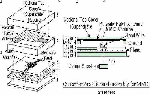
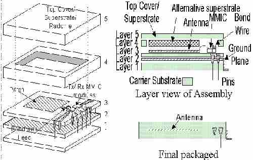
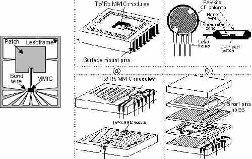
This is a novel method of achieving a complete RF front end product equipped with its radiator within a single chip package. It opens up the opportunity for the designs to be fully integrated in a silicon chip, hence keeping PCB board complexity to the minimum. |
|
||||||||||
This packaging technique provides an alternative solution to problems associated with reduced size antennas implemented on Gallium Arsenide (GaAs) substrates; such as restoration of the antenna gain. This configuration will help to reduce manufacturing cost associated to connecting the antenna with the RF front-end chip. In principle, only the baseband signal, power supply and ground should be needed for such a configuration. |
|||||||||||
NOTE: This is a patent pending solution ..... small is beautiful.....
|
|||||||||||
For further reading: | |||||||||||
1. "Novel antenna for packaged
integrated RF front ends", ISAP2000 conference, Vol. 4C3, pp. 1549-1552,
Fukuoka, Japan, 2000.
|
|||||||||||
2. "Novel packaging
technique for gain enhancement of electrically small antenna designed
on Gallium Arsenide", Electronics Letter Vol 36, No.18, pp1524-1525, 2000
|
|||||||||||
3. "Antenna design for packaged integrated R.F. front ends", IEE colloqium on Integrated small antenna for asset tracking, accepted. |
In recent years, a tremendous amount of research has been geared towards not only miniaturisation of electronic components and its peripherals but also to offer complete system on a single chip, integrating a massive number of components into a single package. Advances in radio frequency integrated circuits(RFIC) are also pushed towards a fully integrated transceiver module. These integrated modules will consist of low noise amplifiers(LNA), mixers, oscillators, phase shifters, passive tuning components, etc. The increasing demand in the wireless communication market has generated the need for compact and fully integrated RF front end products, providing robustness, portability and ease of integration. Whilst these are continuously pursued of optimised RF semiconductor processes, the major challenge now is to incorporate a compact, fully integrated antenna on these transceiver chips. However, these approach for antennas integration are fundamentally limited by their size and hence operating frequency. Our proposal will be aimed at solving these fundamental problems, providing a solution to a truly compact, robust and efficient transceiver chip. |
![]() |
Concept 1 uses an electrically small feed antenna designed on the semiconductor substrate. Hence in principle, this antenna shares a common semiconductor estate with the RF front end circuits. The poor performance of this electrically small antenna is then restore using a parasitic antenna which is place in close proximity to it. In this case, an advantage is that connection from the circuit to the radiator is simplified, hence cutting production costs
|
||
![]() |
Concept 2 uses the substrate properties of the carrier to effectively reduce electrical size of the antenna. Performance of the antenna is then restored through means of dielectric superstrate material, which could be the top cover sealing the entire package. These methods of gain enhancement have been well documented.
|
||
|
In principle, various forms of antennas could be used in such application. The patch antenna shape can be integral with the leadframe and produced by the same process. The support for the patch attached at voltage zeros. some of the other possible packaging design. Figor example, a loop antenna build on a flat pack carrier, a parasitic coupled circular polarisation antenna, a Yagi antenna on the chip carrier and quarter wave H antenna where the MMIC chips are house within the groves of the H structure. Shorting pins, strip line circuits and aperture couple antenna are also possible design prospects. |
![]() |
![]() |
Although dielectric loading and adding of shorting pins are commonly used technique for size reduction of an antenna, structural perturbation are often required to further reduce this physical dimension while maintaining electrical length. For example, by reducing the dimension of the center stem (DY) of the quarter-wave patch to a H shaped antenna. The response of frequency reduction with respect to DY variation are experimentally determined shown on the right graph. However, further size reduction can also be achieved by reducing the number of shorting pins. Operating at 2.46GHz with only 2 shorting pins, the antenna has an overall length and width of 7.5 x 9.8mm. Comparing to the quarter-wave patch antenna, this antenna has an overall area reduction of 3.29 times. This could be very significant as some semiconductor estate could still be expensive. As expected, the gain of these antennas are poor and will be describe in the following section. Note that these antennas are designed on FR4 substrate of 0.5mm thickness. |